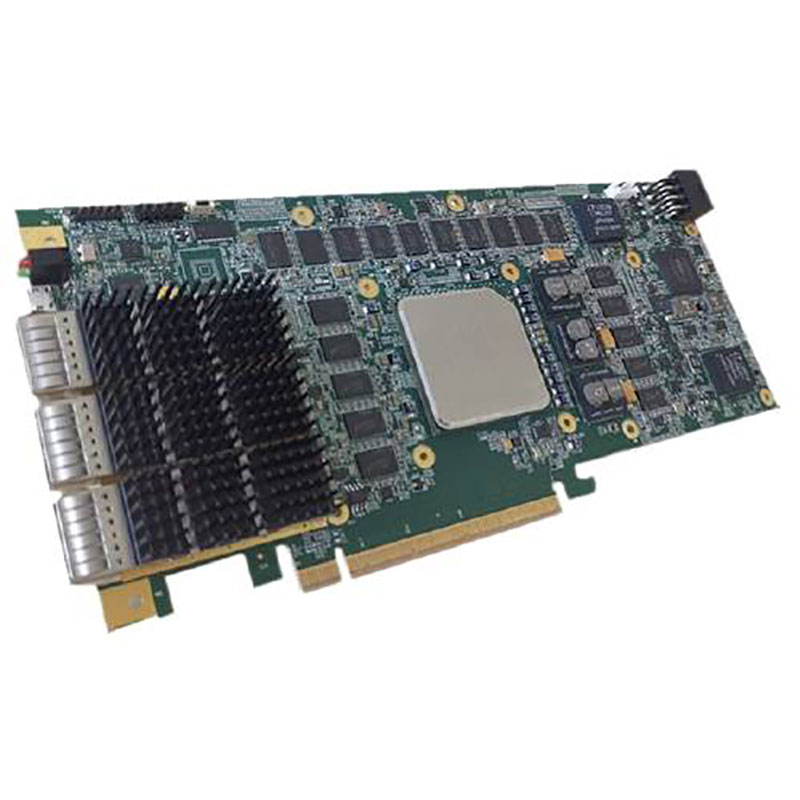
Описание:
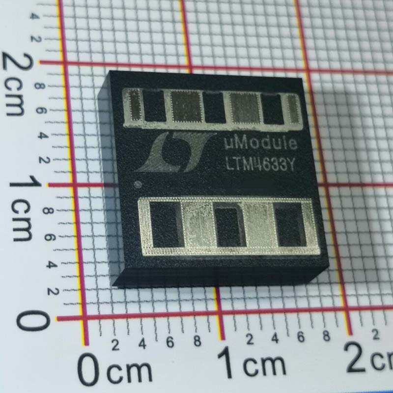
The LTM4633IY#PBF μModule® (power module) regulator combines three complete 10A switching mode DC/DC converters into one small package. Included in the package are the switching controllers, power FETs, inductors, and most support components. The LTM4633IY#PBF’s three regulators operate from 4.7V to 16V input rail(s) or 2.375V to 16V with an external 5V bias. The VOUT1 and VOUT2 output range is 0.8V to 1.8V, while the VOUT3 output range is 0.8V to 5.5V. Each output is set by one external resistor.
High switching frequency and a current mode architecture enable a very fast transient response to line and load changes without sacrificing stability. The device supports frequency synchronization, multiphase parallel operation of VOUT1 and VOUT2, soft-start and output voltage tracking for supply rail sequencing.
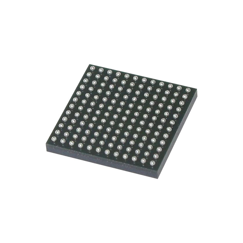
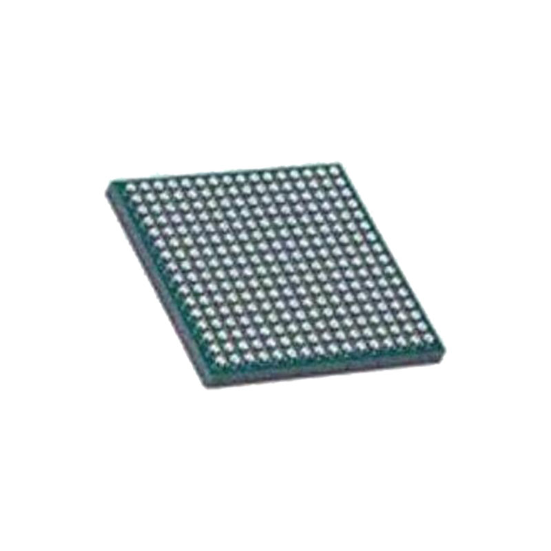
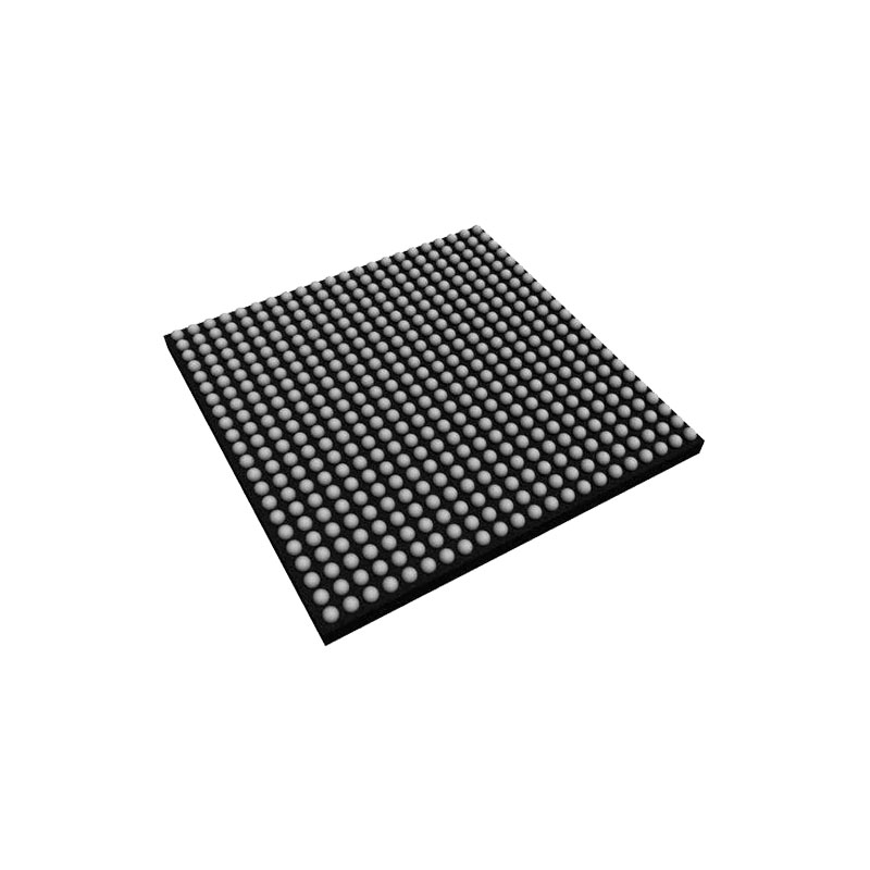
Overcurrent protection,fault protection features include overvoltage protection and temperature monitoring. The power module is offered in a space saving, thermally enhanced 15mm × 15mm × 5.01mm BGA package. The LTM4633IY#PBF is RoHS compliant with Pb-free finish.
Особенности:
Three Independent 10A DC Output Current Regulator Channels
Input Voltage Range: 4.7V to 16V
2.375V to 16V with External 5V Bias
VOUT1,2 Voltage Range: 0.8V to 1.8V
VOUT3 Voltage Range: 0.8V to 5.5V
±1.5% Maximum Total DC Output Error
Управление в режиме тока/быстрая переходная характеристика
Frequency Synchronization
Output Overvoltage and Overcurrent Protection
Multiphase Operation with Current Sharing on VOUT1 and VOUT2
General Purpose Temperature Monitors
Soft-Start/Voltage Tracking
Power Good Monitors
15mm × 15mm × 5.01mm BGA Package
Приложения:
Telecom, Networking and Industrial Equipment,High Density Point of Load Regulation
Pin Functions
GND (A4, A8-A9, D1- D12, E1-E12, F4, F8, F12, G3-G4, G7-G8, G11-G12, H3-H4, H7-H8, H11-H12, J1-J5, J7, J9-J12, K1-K3, K8-K10, K12,L1-L2,L12, M1, M6-M8, M12): Ground Pins for Both Input and Output Returns. All ground pins need to connect with large copper areas underneath the unit.
VOUT1, VOUT2, VOUT3 (A10-A12, B9-B12, and C10-C12); (A5-A7, B5-B8, C6-C8); (A1-A3, B1-B4, C1-C4): Power Output Pins. Apply output load between these pins and the GND pins. Recommend placing output decoupling capacitance directly between these pins and the GND pins. See Table 5. TEMP1 AND TEMP2 (C9, C5): Two Onboard Temperature Diodes for Monitoring the VBE Junction Voltage Change with Temperature. Each of these two temperature diode connected PNP transistors is placed in the middle of channel 1 and channel 2, and in the middle of channel 2 and channel 3. See the Applications Information section and an example in Figure 19.
VIN1,VIN2,VIN3(F9-F10,G9-G10,H9-H10);(F5-F6,G5-G6,H5-H6);(F1-F2,G1-G2,H1-H2): Power Input Pins. Apply input voltage between these pins and the GND pins. Recommend placing input decoupling capacitance directly between the VIN pins and the GND pins. The VIN paths can be all combined from one power source, or powered from independent power sources. The VIN paths can operate down to 2.375V when the CNTL_PWR is biased separately from a supply in the range of 4.7V to 16V. See the Applications Information section.
SW1 (F11), SW2 (F7), SW3 (F3): The internal switch node for each of the regulator channels for monitoring the switching waveform. An R-C snubber circuit can be placed on these pins to ground to eliminate switch node ringing noise.
CNTL_PWR (J6): Input Supply to an Internal Bias LDO to Power the Internal Controller and MOSFET Drivers. This pin is connected to an input supply voltage range of 4.7V to 16V. If the voltage at CNTL_PWR is ≤5.5V, the INTVCC pin should be tied to CNTL_PWR for optimum efficiency. If the voltage at CNTL_PWR is >5.5V, leave INTVCC floating with the recommended decoupling capacitor. When using multiple input supplies, choose the lowest input supply between 4.7V to 16V to supply the CNTL_PWR pin. This will lower the internal power loss and improve efficiency.
INTVCC (J8): Output of the Internal Bias LDO for Powering Internal Control Circuitry. Connect a 4.7µF ceramic capacitor to ground for decoupling. If the voltage at CNTL_PWR is ≤5.5V, tie the INTVCC pin to CNTL_PWR for optimum efficiency. If the voltage at CNTL_PWR is >5.5V, leave INTVCC floating. See the Applications Information section.
SGND (K6-K7, L6-L7): Signal Ground Connections. The signal ground connection in the module is separated from normal power ground (GND) by an internal 2.2Ω resistor. This allows the designer to connect the signal ground pin close to GND near the external output capacitors on the regulator channel’s outputs. The entire internal small-signal feedback circuitry is referenced to SGND, thus allowing for better output regulation. See the recommended layout in the Applications Information section.
EXTVCC (L3): External Bias Power Input. The internal bias LDO is bypassed whenever the voltage at EXTVCC is above 4.7V. Never exceed 6V at this pin and ensure CNTL_PWR > EXTVCC at all times to avoid reverse polarity on the internal bias LDO. Connect a 1µF capacitor to ground when used otherwise leave floating. When generating a 5V output on channel 3, connect the 5V output to this pin to improve efficiency.

