Описание:
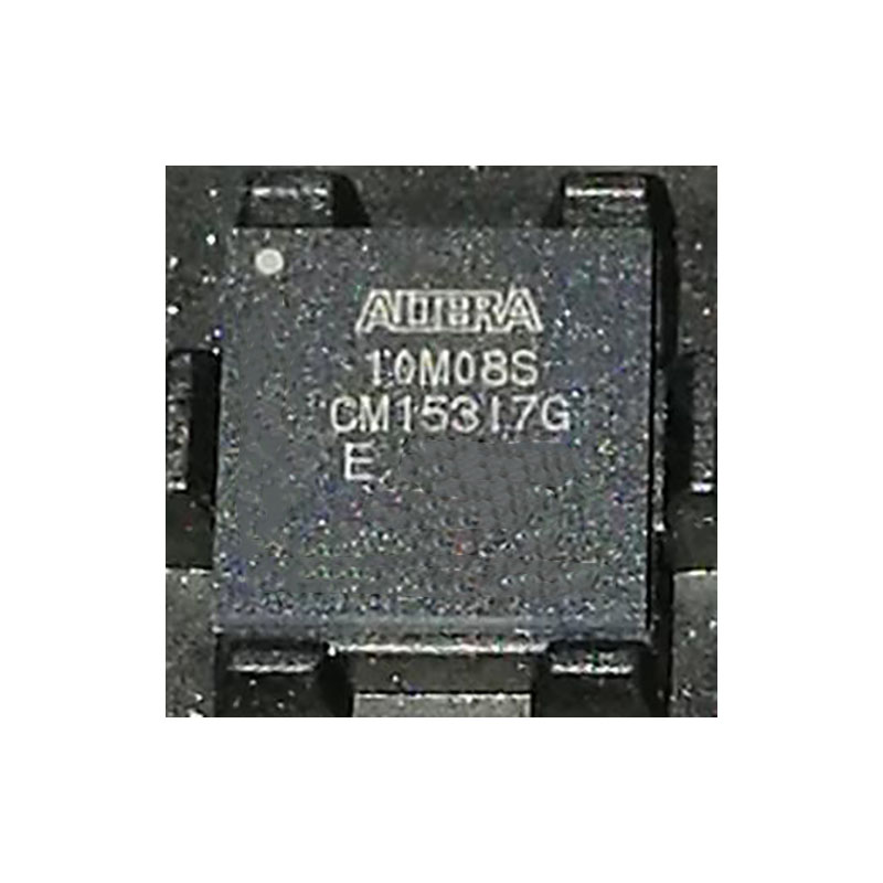
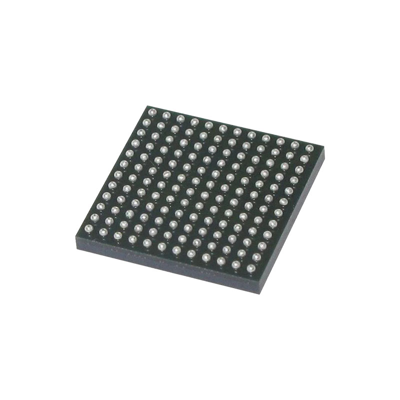
The Product 10M08SCM153I7G belongs to INTEL’s MAX ® 10 FPGA series.
In order to achieve low static power consumption, the core structural architecture of this series adopts a low static power consumption architecture, which is based on optimized 55 nanometer flash memory technology.
The product has flexibility and integration, with a single device integrating non-volatile flash memory, programmable logic devices (PLDs), random access memory (RAM), digital signal processing (DSP), DDR3 external memory interface, analog-to-digital converter (ADC), phase-locked loop (PLL), and various I/O standards in a small 3mm x 3mm package.
With a simple and quick configuration method, device configuration can be completed in less than 10 milliseconds on a secure on-chip flash memory.
The highlights of the Intel MAX 10 devices include:
• Internally stored dual configuration flash
• User flash memory
• Instant on support
• Integrated analog-to-digital converters (ADCs)
• Single-chip Nios II soft core processor support
Приложения:
The Product are the ideal solution for system management, I/O expansion, communication control planes, industrial, automotive, and consumer applications.
Key Advantages of Intel MAX 10 Devices
Simple and fast configuration:
Secure on-die flash memory enables device configuration in less than 10 ms
Flexibility and integration:
Single device integrating PLD logic, RAM, flash memory, digital signal processing (DSP), ADC, phase-locked loop (PLL), and I/Os
Small packages available from 3 mm × 3 mm
Low power
Sleep mode—significant standby power reduction and resumption in less than 1 ms
Longer battery life—resumption from full power-off in less than 10 ms
20-year-estimated life cycle
Built on TSMC’s 55 nm embedded flash process technology
High productivity design tools
Intel Quartus® Prime Lite edition (no cost license)
Platform Designer (Standard) system integration tool
DSP Builder for Intel FPGAs
Nios® II Embedded Design Suite (EDS)
Технология
55 nm TSMC Embedded Flash (Flash + SRAM) process technology
Упаковка
Low cost, small form factor packages—support multiple packaging technologies and pin pitches
Несколько плотностей устройств с совместимыми размерами корпусов для беспрепятственной миграции между различными плотностями устройств
RoHS6-compliant
Архитектура ядра
4-input look-up table (LUT) and single register logic element (LE)
LEs arranged in logic array block (LAB)
Embedded RAM and user flash memory
Clocks and PLLs
Встроенные блоки умножения
General purpose I/Os
Внутренние блоки памяти
M9K—9 kilobits (Kb) memory blocks
Cascadable blocks to create RAM, dual port, and FIFO functions
User flash memory (UFM)
User accessible non-volatile storage
High speed operating frequency
Large memory size
High data retention
Multiple interface option
Встроенные блоки умножения
One 18 × 18 or two 9 × 9 multiplier modes
Cascadable blocks enabling creation of filters, arithmetic functions, and image processing pipelines
ADC
12-bit successive approximation register (SAR) type
Up to 17 analog inputs
Cumulative speed up to 1 million samples per second ( MSPS)
Integrated temperature sensing capability
Часовые сети
Global clocks support
High speed frequency in clock network
Internal oscillator
Built-in internal ring oscillator
PLLs
Analog-based
Low jitter
High precision clock synthesis
Clock delay compensation
Zero delay buffering
Multiple output taps
Входы/выходы общего назначения (GPIO)
Поддержка нескольких стандартов ввода/вывода
Оконечное устройство на кристалле (OCT)
Up to 720 megabits per second (Mbps) LVDS receiver and transmitter
External memory interface (EMIF)
Supports up to 600 Mbps external memory interfaces:
DDR3, DDR3L, DDR2, LPDDR2 (on 10M16, 10M25, 10M40, and 10M50.)
SRAM (Hardware support only)
Note:
EMIF is only supported in selected Intel MAX 10 device density and package combinations.Refer to the External Memory Interface User Guide for more information.
For 600 Mbps performance, –6 device speed grade is required. Performance varies according to device grade (commercial, industrial, or automotive) and device speed grade (–6 or –7). Refer to the Intel MAX 10 FPGA Device Datasheet or External Memory Interface Spec Estimator for more details.
Конфигурация
Internal configuration
JTAG
Advanced Encryption Standard (AES) 128-bit encryption and compression options
Flash memory data retention of 20 years at 85 °C
Flexible power supply schemes
Single- and dual-supply device options
Dynamically controlled input buffer power down
Sleep mode for dynamic power reduction
Feature Options for Intel MAX 10 Devices
Compact
Devices with core architecture featuring single configuration image with self-configuration capability
Flash
Devices with core architecture featuring:
Dual configuration image with self-configuration capability
Remote system upgrade capability
Memory initialization
Аналог
Devices with core architecture featuring:
Dual configuration image with self-configuration capability
Remote system upgrade capability
Memory initialization
Integrated ADC

