ОБЩЕЕ ОПИСАНИЕ
The AD5560 is a high performance, highly integrated device power supply consisting of programmable force voltages and measure ranges. This part includes the required DAC levels to set the programmable inputs for the drive amplifier, as well as clamping and comparator circuitry. Offset and gain correction is included on-chip for DAC functions. A number of programmable measure current ranges are available: five internal fixed ranges and two external customer-selectable ranges (EXTFORCE1 and EXTFORCE2) that can supply currents up to ±1.2 A and ±500 mA, respectively.
The voltage range possible at this high current level is limited by headroom and the maximum power dissipation. Current ranges in excess of ±1.2 A or at high current and high voltage combinations can be achieved by paralleling or ganging multiple DPS devices.Open-drain alarm outputs are provided in the event of over current,over temperature, or Kelvin alarm on either the SENSE or DUTGND line.
The DPS functions are controlled via a simple 3-wire serial interface compatible with SPI, QSPI™, MICROWIRE™, and DSP interface standards running at clock speeds of up to 50 MHz.
ОСОБЕННОСТИ
► Programmable device power supply (DPS)
► FV, MI, MV, FNMV functions
► 5 internal current ranges (on-chip RSENSE)
► ±5 µA, ±25 µA, ±250 µA, ±2.5 mA, ±25 mA
► 2 external high current ranges (external RSENSE)
► EXTFORCE1: ±1.2 A maximum
► EXTFORCE2: ±500 mA maximum
► Integrated programmable levels
► All 16-bit DACs: force DAC, comparator DACs, clamp DACs,offset DAC, OSD DAC, DGS DAC
► Programmable Kelvin clamp and alarm
► Offset and gain correction registers on-chip
► Ramp mode on force DAC for power supply slewing
► Programmable slew rate feature, 1 V/μs to 0.3 V/μs
► DUTGND Kelvin sense and alarm
► 25 V FV span with asymmetrical operation within −22 V/+25 V
► On-chip comparators
► Gangable for higher current
► Guard amplifier
► System PMU connections
► Current clamps
► Die temperature sensor and shutdown feature
► On-chip diode thermal array
► Diagnostic register allows access to internal nodes
► Open-drain alarm flags (temperature, current clamp, Kelvinalarm)
► SPI-/MICROWIRE-/DSP-compatible interface
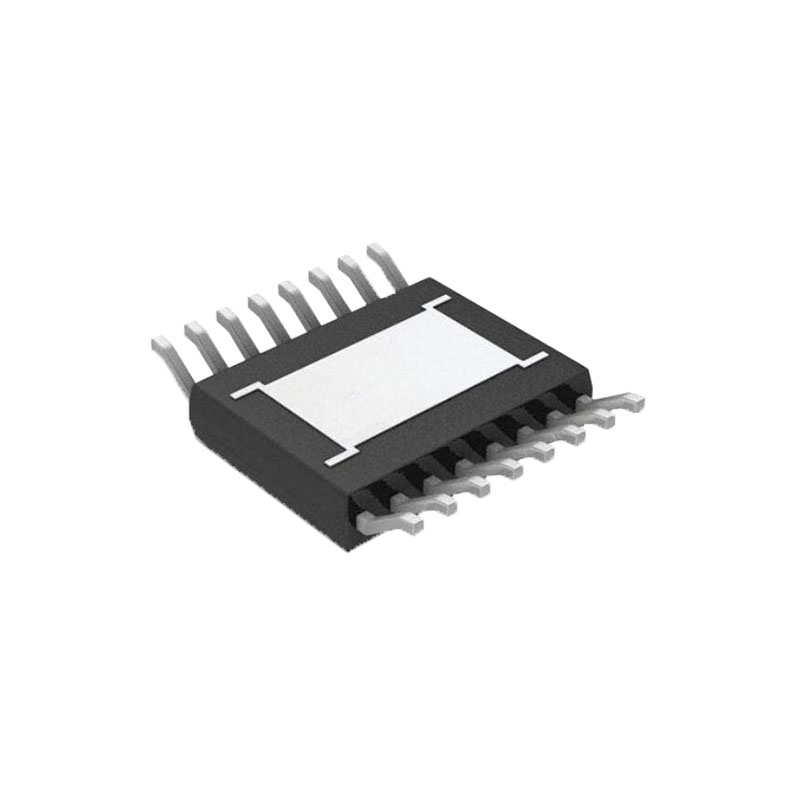
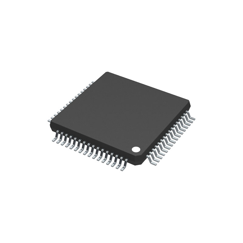
► 64-lead (10 mm × 10 mm) TQFP with exposed pad (on top)
► 72-ball (8 mm × 8 mm) flip-chip BGAAPPLICATIONS
► Automatic test equipment (ATE)
► Device power supply
ТЕРМИНОЛОГИЯ
Ошибка смещения
Offset error is a measure of the difference between the actual voltage and the ideal voltage at midscale or at zero current expressed in millivolts (mV) or percentage of full-scale range (%FSR).
Ошибка усиления
Gain error is the difference between full-scale error and zero-scale error. It is expressed in percentage of full-scale range (%FSR).
Gain Error = Full-Scale Error − Zero-Scale Error
where: Full-Scale Error is the difference between the actual voltage and the ideal voltage at full scale. Zero-Scale Error is the difference between the actual voltage and the ideal voltage at zero scale.
Linearity Error
Linearity error, or endpoint linearity, is a measure of the maximum deviation from a straight line passing through the endpoints of the full-scale range. It is measured after adjusting for offset error and gain error and is expressed in millivolts (mV).
Common-Mode (CM) Error
CM error is the error at the output of the amplifier due to the common-mode input voltage. It is expressed in percentage of full-scale voltage range per volt (%FSVR/V).
Clamp Limit
Clamp limit is a measure of where the clamps begin to function fully and limit the clamped voltage or current.
Leakage Current
Leakage current is the current measured at an output pin when the circuit connected to that pin is in high impedance state.
Slew Rate
The slew rate is the rate of change of the output voltage expressed in volts per microsecond (V/μs).
Differential Nonlinearity DNL
DNL is the difference between the measured change and the ideal 1 LSB change between any two adjacent codes. A specified DNL of ±1 LSB maximum ensures monotonicity.
Время установления выходного напряжения
Output voltage settling time is the amount of time it takes for the output of a DAC to settle to a specified level for a full-scale input change.
Digital-to-Analog Glitch Energy
Digital-to-analog glitch energy is the amount of energy that is injected into the analog output at the major code transition. It is specified as the area of the glitch in nanovolts per second (nV-sec).
It is measured by toggling the DAC register data between 0x7FFF and 0x8000.
Коэффициент отклонения сигнала источника питания переменного тока (ACPSRR)
ACPSRR is a measure of the part’s ability to avoid coupling noise and spurious signals that appear on the supply voltage pin to the output of the switch. The dc voltage on the device is modulated by a sine wave of 0.2 V p-p. The ratio of the amplitude of the signal on the output to the amplitude of the modulation is the ACPSRR. It is expressed in decibels (dB).
VSTRESS
VSTRESS is the stress voltage applied to each pin during leakage testing.
ТЕОРИЯ ЭКСПЛУАТАЦИИ
The AD5560 is a single-channel, device power supply for use in semiconductor automatic test equipment. All the DAC levels required to operate the device are available on chip.
This device contains programmable modes to force a pin voltage and measure the corresponding current (FVMI) covering a wide current measure range of up to ±1.2 A. A voltage sense amplifier allows measurement of the DUT voltage. Measured current or voltage is available on the MEASOUT pin.of analyzing the temperature at different points across the die.