ОБЩЕЕ ОПИСАНИЕ
The AD7547 contains two 12-bit current output DACs on onemonolithic chip.Also on-chip are the level shifters,data registersand control logic for easy microprocessor interfacing.There are12 data inputs.CSA,CSB,WR control DAC selection andloading.Data is latched into the DAC registers on the risingedge of WR.The device is speed compatible with most micro-processors and accepts TTL,74HC and 5V CMOS logic levelinputs.
The D/A converters provide 4-quadrant multiplication capabilitieswith separate reference inputs and feedback resistors.Monolithicconstruction ensures that thermal and gain error tracking isexcellent.12-bit monotonicity is guaranteed for both DACs overthe full temperature range.
The AD7547 is manufactured using the Linear CompatibleCMOS (LC²MOS)process.This allows fast digital logic andprecision linear circuitry to be fabricated on the same die.
ОСНОВНЫЕ ХАРАКТЕРИСТИКИ ПРОДУКЦИИ
1.DAC to DAC Matching
Since both DACs are fabricated on the same chip,precisematching and tracking is inherent.Many applications whichare not practical using two discrete DACs are now possible.Typical matching:0.5%.
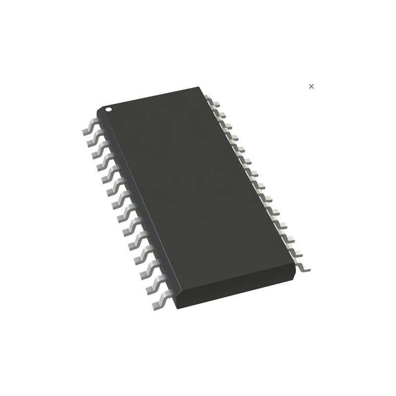
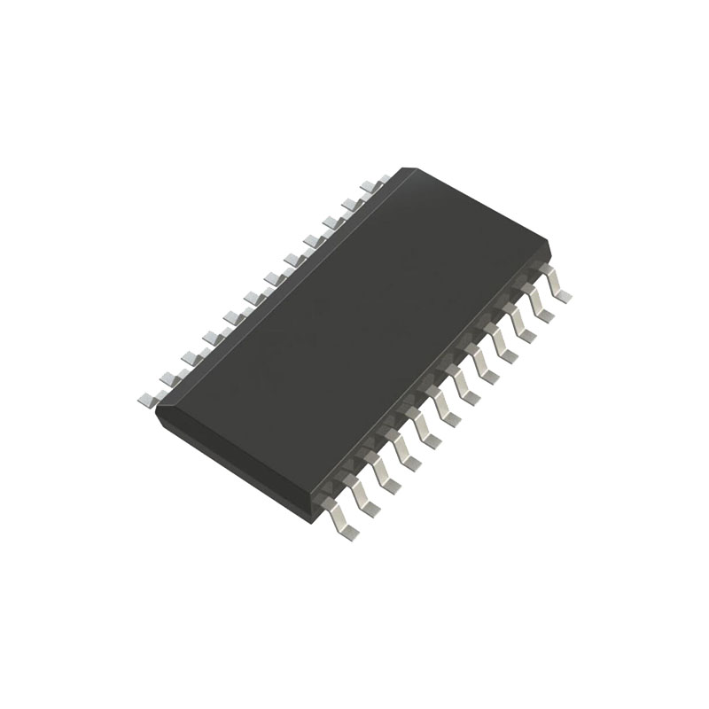
2.Small Package SizeThe AD7547 is available in 0.3″wide 24-pin DIPs and SOICsand in 28-terminal surface mount packages.
3.Wide Power Supply ToleranceThe device operates on a +12V to+15V VDp,with±10%tolerance on this nominal figure.All specifications are guaran-teed over this range.
ОСОБЕННОСТИ
Two 12-Bit DACs in One Package
DAC Ladder Resistance Matching:0.5%
Space Saving Skinny DIP and Surface Mount Packages
- Quadrant MultiplicationLow Gain Error(1LSB max Over Temperature)
- Fast Interface Timing
ПРИЛОЖЕНИЯ
Автоматическое испытательное оборудование
Programmable Filters
Audio Applications
Synchro Applications
Управление процессом
ИНФОРМАЦИЯ О ЦЕПИ
D/A SECTION
The AD7547 contains two identical 12-bit multiplying D/Aconverters.Each DAC consists of a highly stable R-2R ladderand 12 N-channel current steering switches.In the R-2R ladder,binaryweighted currents are steered between IouTA and AGND.Thecurrent flowing in each ladder leg is constant,irrespective ofswitch state.The feedback resistor RFBA is used with an op-amp to convert the current flowing in IouTA toa voltage output.
DIGITAL CIRCUIT INFORMATION
The digital inputs are designed to be both TTL and 5V CMOScompatible.All logic inputs are static-protected MOS gates withtypical input currents of less than InA.
UNIPOLAR BINARY OPERATION(2-QUADRANT MULTIPLICATION)
With an ac input,the circuit performs 2-quadrant multiplication.Operational amplifiers Al and A2 can be in a single package(AD644,AD712)or separate packages(AD544,AD711,AD OP-27).Capacitors Cl and C2 provide phase compensationto help prevent overshoot and ringing when high speed op-ampsare used.For zero offset adjustment,the appropriate DAC register isloaded with all O’s and amplifier offset adjusted so that VouTAor VouTB is OV.Full-scale trimming is accomplished by loadingthe DAC register with all I’s and adjusting R1(R3)so thatVoUTA(VouTB)=-VIN(4095/4096).For high temperatureoperation,resistors and potentiometers should have a low Tem-perature Coefficient.In many applications,because of the excellentGain T.C.and Gain Error specifications of the AD7547,GainError trimming is not necessary.In fixed reference applications,full-scale can also be adjusted by omitting R1,R2,R3,R4 andtrimming the reference voltage magnitude.
APPLICATION HINTS
Output Offset
The maximum amplitude of this error,whichadds to the D/A converter nonlinearity,depends on Vos,whereVos is the amplifier input offset voltage.To maintain specifiedoperation,it is recommended that Vos be no greater than(25×10-6)(VREF)over the temperature range of operation.Suitableop amps are the AD711C and its dual version,the AD712C.These op amps have a wide bandwidth and high slew rate andare recommended for wide bandwidth ac applications.AD711/AD712 settling time to 0.01%is typically Iμs.
Temperature Coefficients
The gain temperature coefficient ofthe AD7547 has a maximum value of 5ppm/C and typical valueof lppm/℃.This corresponds to worst case gain shifts of 2LSBsand 0.4LSBs respectively over a 100℃ temperature range.Whentrim resistors R1(R3)and R2(R4)are used to adjust full-scalerange as in Figure 4,the temperature coefficient of R1(R3)andR2(R4)should also be taken into account.For further informationsee”Gain Error and Gain Temperature Coefficient of CMOSMultiplying DACs”,Application Note,Publication NumberE630c-5-3/86 available from Analog Devices.
High Frequency Considerations
AD7547 output capacitanceworks in conjunction with the amplifier feedback resistance toadd a pole to the open loop response.This can cause ringing oroscllation.Stability can be restored by adding a phase compen-sation capacitor in parallel with the feedback resistor.
Feedthrough
The dynamic performance of the AD7547 dependsupon the gain and phase stability of the output amplifier,togetherwith the optimum choice of PC board layout and decouplingcomponents.