PRODUCT DESCRIPTION
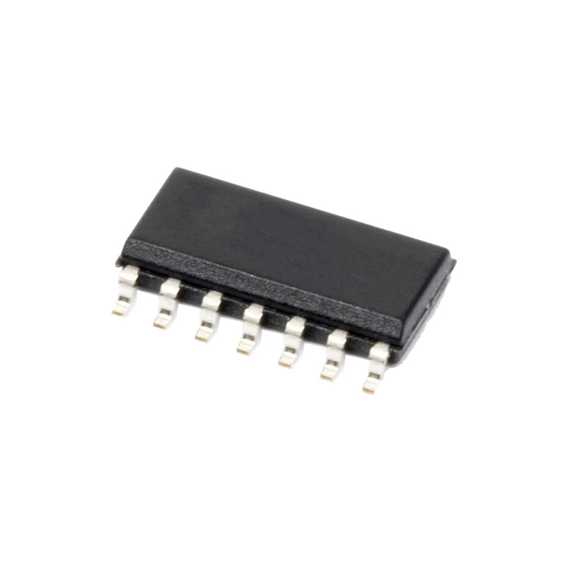
The AD8184 is a high speed 4-to-1 multiplexer. It offers –3 dB signal bandwidth of 700 MHz along with a slew rate of 750 V/µs. With 95 dB of crosstalk and 115 dB isolation, it is useful in many high speed applications. The differential gain and differential phase error of 0.01% and 0.01°, along with 0.1 dB flatness of 75 MHz, make AD8184 ideal for professional video multiplexing. It offers 10 ns switching time, making it an excellent choice for pixel switching (picture-in-picture) while consuming less than 4.5 mA on ±5 V supply voltage. The AD8184 offers a high speed disable feature allowing the output to be put into a high impedance state. This allows multiple outputs to be connected together for cascading stages while the “OFF” channels do not load the output bus. It operates on voltage supplies of ±5 V and is offered in 14-lead PDIP and SOIC packages.
ОСОБЕННОСТИ
Single and Dual 2-to-1 Also Available (AD8180 and AD8182)
Fully Buffered Inputs and Outputs
Fast Channel Switching: 10 ns
Высокая скорость
> 700 MHz Bandwidth (–3 dB)
> 750 V/ s Slew Rate
Fast Settling Time of 15 ns to 0.1%
Excellent Video Specifications (RL > 2 k )
Gain Flatness of 0.1 dB of 75 MHz
0.01% Differential Gain Error, RL = 10 k
0.01 Differential Phase Error, RL = 10 k
Low Power: 4.4 mA
Low Glitch: < 25 mV
Low All-Hostile Crosstalk of –95 dB @ 5 MHz
High “OFF” Isolation of –115 dB @ 5 MHz
Low Cost
Fast Output Disable Feature for Connecting Multiple Devices
ПРИЛОЖЕНИЯ
Pin Compatible with HA4314* and GX4314*
Video Switchers and Routers
Pixel Switching for “Picture-In-Picture”
Switching in LCD and Plasma Displays
ТЕОРИЯ ЭКСПЛУАТАЦИИ
The AD8184 video multiplexer is designed for fast switching (10 ns) and wide bandwidth (> 700 MHz). This performance is attained with low power dissipation (4.4 mA, enabled) through the use of proprietary circuit techniques and a dielectricallyisolated complementary bipolar process. This device has a fast disable function that allows the outputs of several muxes to be wired in parallel to form a larger mux with little degradation in switching time. The low disabled output capacitance (3.2 pF) helps to preserve the system bandwidth in larger matrices. Unlike earlier CMOS switches, the switched open-loop buffer architecture of the AD8184 provides a unidirectional signal path with minimal switching glitches and constant, low input capacitance. Since the input impedance of these muxes is nearly independent of the load impedance and the state of the mux, the frequency response of the ON channels in a large switch matrix is not affected by fanout.The decoder logic translates TTLcompatible logic inputs (A0, A1 and ENABLE) to internal, differential ECL levels for fast, low-glitch switching. The A0 (LSB) and A1 (MSB) control inputs constitute a two-bit binary word that determines which of the four buffers is enabled, unless the ENABLE input is HIGH, in which case all buffers are disabled and the output is switched to a high impedance state. Each open-loop buffer is implemented as a complementary emitter follower that provides high input impedance, symmetric slew rate and load drive, and high output-to-input isolation due to its β2 current gain. The selected buffer is biased ON by fast switched current sources that allow the buffer to turn on quickly. Dedicated flatness circuits, combined with the open-loop architecture of the AD8184, keep peaking low (typically < 0.5 dB) when driving high capacitive loads, without the need for external series resistors at the input or output. If better flatness response is desired, an input series resistance (RS) may be used although this will increase crosstalk. The dc gain of the AD8184 is almost independent of load for RL > 10 kΩ. For heavier loads, the dc gain is approximately that of the voltage divider formed by the output impedance of the mux (typically 28 Ω and RL). High speed disable clamp circuits (not shown) at the bases of Q3 and Q4 allow the buffers to turn off quickly and cleanly without dissipating much power once off. Moreover, these clamps shunt displacement currents flowing through the junction capacitances of Q1 and Q2 away from the bases of Q3 and Q4 and to ac ground through low impedances. The two-pole high-pass frequency response of the T switch formed by these clamps is a significant improvement over the one-pole high pass response of a simple series CMOS switch. As a result, board and package parasitics, especially stray capacitance between inputs and outputs, may limit the achievable crosstalk and off isolation.