ОБЩЕЕ ОПИСАНИЕ
ADP7159 - регулируемый линейный регулятор, работающий от 2,3 В до 5,5 В и обеспечивающий выходной ток до 2 А. В зависимости от модели возможно выходное напряжение от 1,2 В до 3,3 В. Используя передовую фирменную архитектуру, устройство обеспечивает высокое отклонение по питанию и сверхнизкий уровень шума, достигая превосходной переходной характеристики линии и нагрузки при использовании только керамического выходного конденсатора 10 мкФ.
ADP7159 выпускается в четырех моделях, которые оптимизируют рассеиваемую мощность и PSRR в зависимости от входного и выходного напряжения. Руководства по выбору см. в таблицах 9 и 10.
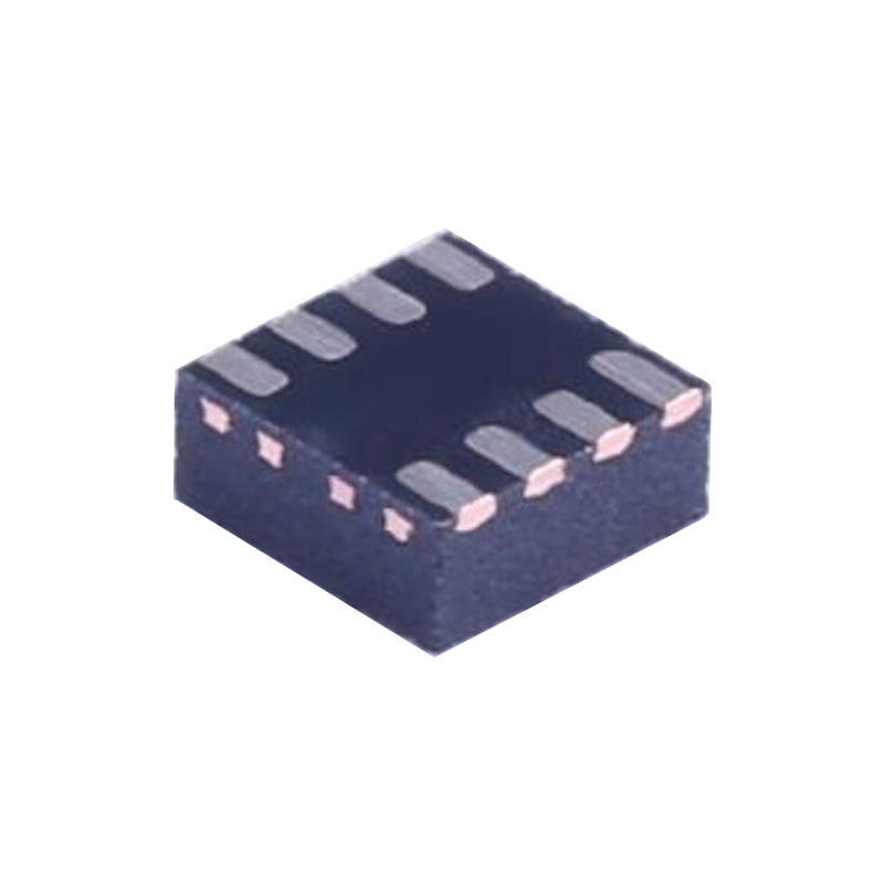
Типичный выходной шум регулятора ADP7159 составляет 0,9 мкВ rms от 100 Гц до 100 кГц и 1,7 нВ/√Гц для спектральной плотности шума от 10 кГц до 1 МГц. ADP7159 выпускается в 10-выводных корпусах LFCSP 3 мм×3 мм и 8-выводных корпусах SOIC, что делает его не только очень компактным решением, но и обеспечивает отличные тепловые характеристики для приложений, требующих выходного тока до 2 А при малом и низкопрофильном корпусе.
ТЕРМАЛЬНЫЕ ДАННЫЕ
Абсолютные максимальные значения применяются только по отдельности, но не в комбинации. ADP7159 может быть поврежден при превышении предельной температуры спая. Контроль температуры окружающей среды не гарантирует, что TJ находится в указанных температурных пределах. В приложениях с высокой рассеиваемой мощностью и низкой термостойкостью максимальная температура окружающей среды может быть уменьшена.
В приложениях с умеренной рассеиваемой мощностью и низким тепловым сопротивлением печатной платы максимальная температура окружающей среды может превышать максимальный предел, если температура спая находится в пределах спецификации. Температура спая (TJ) устройства зависит от температуры окружающей среды (TA), рассеиваемой мощности устройства (PD) и теплового сопротивления спая и окружающей среды корпуса (θJA).
ТЕОРИЯ ЭКСПЛУАТАЦИИ
ADP7159 - линейный регулятор с ультранизким уровнем шума и высоким PSRR, предназначенный для радиочастотных приложений. Диапазон входных напряжений составляет от 2,3 В до 5,5 В, устройство обеспечивает ток нагрузки до 2 А. Типичный ток потребления при выключении составляет 0,2 мкА при комнатной температуре.
Оптимизированный для использования с керамическими конденсаторами емкостью 10 мкФ, ADP7159 обеспечивает превосходные переходные характеристики.
Внутри ADP7159 состоит из опорного, усилителя ошибки и P-канального MOSFET транзистора.Выходной ток подается через PMOS транзистор, который управляется усилителем ошибки.Усилитель ошибки сравнивает опорное напряжение с напряжением обратной связи с выхода и усиливает разницу.Если напряжение обратной связи ниже опорного напряжения, затвор PMOS транзистора опускается, позволяя большему току проходить и увеличивая выходное напряжение.Если напряжение обратной связи выше опорного напряжения, затвор PMOS-прибора подтягивается выше, позволяя меньшему току проходить и уменьшая выходное напряжение. Благодаря сильной фильтрации опорного напряжения ADP7159 достигает типичного выходного сигнала 1,7 нВ/√Гц в диапазоне от 10 кГц до 1 МГц. Поскольку усилитель ошибки всегда находится в режиме единичного усиления, выходной шум не зависит от выходного напряжения.
ВЫБОР КОНДЕНСАТОРА
Многослойные керамические конденсаторы (MLCC) сочетают в себе малый размер, низкий ESR, низкую эффективную последовательную индуктивность (ESL) и широкий диапазон рабочих температур, что делает их идеальным выбором для шунтирования
Однако они не лишены недостатков. В зависимости от материала диэлектрика, емкость может сильно меняться в зависимости от температуры, постоянного напряжения и уровня сигнала переменного тока. Поэтому выбор правильного конденсатора приводит к наилучшим характеристикам схемы.
Выходной конденсатор
Выходной конденсатор ADP7159 предназначен для работы с керамическими конденсаторами, но при соблюдении осторожности в отношении значения ESR он может работать с наиболее распространенными конденсаторами. ESR выходного конденсатора влияет на стабильность контура управления LDO. Для обеспечения стабильности работы ADP7159 рекомендуется использовать емкость не менее 10 мкФ с ESR не более 0,2Ω. Выходная емкость также влияет на переходный отклик на изменение тока нагрузки. Использование большего значения выходной емкости улучшает переходный отклик ADP7159 на большие изменения тока нагрузки.
Защита от предельного тока и теплового отключения предназначена для защиты устройства от случайных перегрузок. Случаи с жестким замыканием VOUT на землю или очень длинным таймером плавного пуска обычно приводят к тепловым колебаниям устройства между предельным током и тепловым отключением.