ОСОБЕННОСТИ
Ultrawideband frequency range: 9 kHz to 40 GHz
Attenuation range: 0.5 dB steps to 31.5 dB
Low insertion loss with impedance match
2.0 dB up to 18 GHz
2.8 dB up to 26 GHz
4.5 dB up to 40 GHz
Attenuation accuracy with impedance match
±(0.20 + 1.0% of attenuation state) up to 18 GHz
±(0.20 + 1.5% of attenuation state) up to 26 GHz
±(0.40+ 3.0% of attenuation state) up to 40 GHz
Typical step error with impedance match
±0.25 dB up to 26 GHz
±0.65 dB up to 40 GHz
High input linearity
P0.1dB insertion loss state: 30 dBm
P0.1dB other attenuation states: 27 dBm
IP3: 50 dBm typical
High RF input power handling: 27 dBm average, 30 dBm peak
Tight distribution in relative phase
No low frequency spurious signals
SPI and parallel mode control, CMOS/LVTTL compatible
RF amplitude settling time (0.1 dB of final RF output): 8 µs
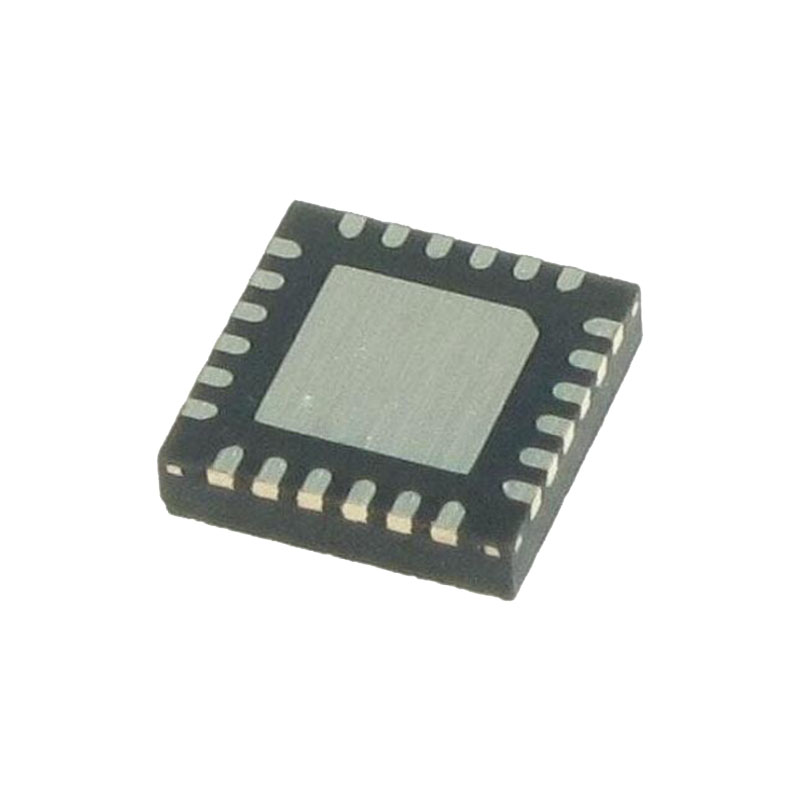
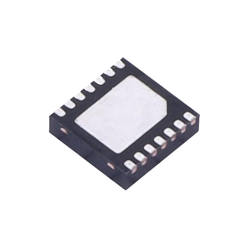
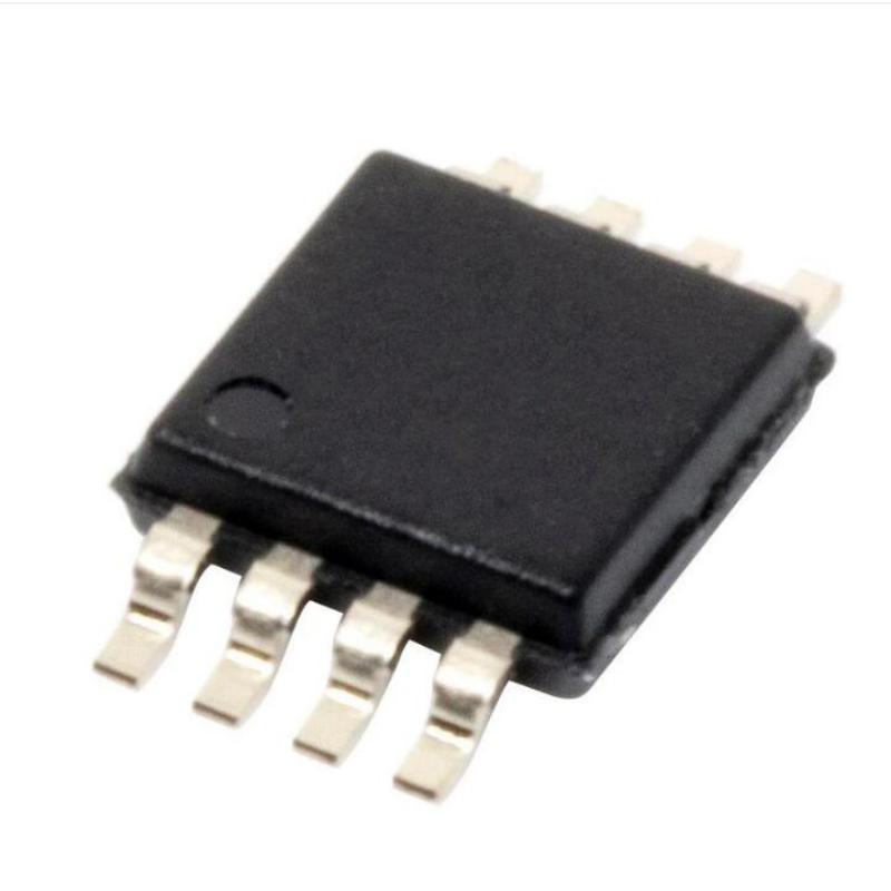
24-terminal, 4 mm × 4 mm LGA package
Pin-compatible with ADRF5730, fast switching version
ПРИЛОЖЕНИЯ
Industrial scanners
Test and instrumentation
Cellular infrastructure: 5G millimeter wave
Military radios, radars, electronic counter measures (ECMs)
Микроволновые радиостанции и терминалы с очень малой апертурой (VSAT)
ОБЩЕЕ ОПИСАНИЕ
The ADRF5720 is a silicon, 6-bit digital attenuator with 31.5 dB attenuation control range in 0.5 dB steps.
This device operates from 9 kHz to 40 GHz with better than 4.5 dB of insertion loss and excellent attenuation accuracy. The ATTIN port of the ADRF5720 has a radio frequency (RF) input power handling capability of 27 dBm average and 30 dBm peak for all states.
The ADRF5720 requires a dual supply voltage of +3.3 V and −3.3 V. The device features serial peripheral interface (SPI), parallel mode control, and complementary metal-oxide semiconductor (CMOS)-/low voltage transistor to transistor logic (LVTTL)-compatible controls.
The ADRF5720 is pin-compatible with the ADRF5730, the fast switching version, which operates from 100 MHz to 40 GHz.
The ADRF5720 RF ports are designed to match a characteristic impedance of 50 Ω. For wideband applications, impedance matching on the RF transmission lines can further optimize high frequency insertion loss, return loss, and attenuation accuracy characteristics. Refer to the Electrical Specifications section, the Typical Performance Characteristics section, and the Applications Information section for more details.
The ADRF5720 comes in a 24-terminal, 4 mm × 4 mm, RoHS compliant, land grid array (LGA) package and operates from −40°C to +105°C.
ТЕОРИЯ ЭКСПЛУАТАЦИИ
The ADRF5720 incorporates a 6-bit fixed attenuator array that offers an attenuation range of 31.5 dB in 0.5 dB steps. An integrated driver provides both serial and parallel mode control of the attenuator array.
POWER SEQUENCE
Bypassing capacitors are recommended on the positive supply voltage line (VDD) and negative supply line (VSS) to filter high frequency noise.
The power-up sequence is as follows:
- Connect GND.
- Power up the VDD and VSS voltages. Power up VSS after VDD to avoid current transients on VDD during ramp-up.
- Power up the digital control inputs. The order of the digital control inputs is not important. However, powering the digital control inputs before the VDD voltage supply may inadvertently forward bias and damage the internal ESD structures. To avoid this damage, use a series 1 kΩ resistor to limit the current flowing in to the control pin. Use pullup or pull-down resistors if the controller output is in a high impedance state after the VDD voltage is powered up and the control pins are not driven to a valid logic state.
- Apply an RF input signal to ATTIN or ATTOUT.
- The power-down sequence is the reverse order of the power-up sequence.
Power-Up State
The ADRF5720 has internal power-on reset circuity. This circuity sets the attenuator to the maximum attenuation state (31.5 dB) when the VDD and VSS voltages are applied and LE is set to low.
RF INPUT AND OUTPUT
Both RF ports (ATTIN and ATTOUT) are dc-coupled to 0 V. No dc blocking is required at the RF ports when the RF line potential is equal to 0 V.
The RF ports are internally matched to 50 Ω. Therefore, external matching components are not required. For wideband applications, use impedance matching to improve insertion loss, return loss, and attenuation accuracy performance at high frequencies.
The ADRF5720 supports bidirectional operation at a lower power level. The power handling of the ATTIN and ATTOUT ports are different. Therefore, the bidirectional power handling is defined by the ATTOUT port.

