ОПИСАНИЕ
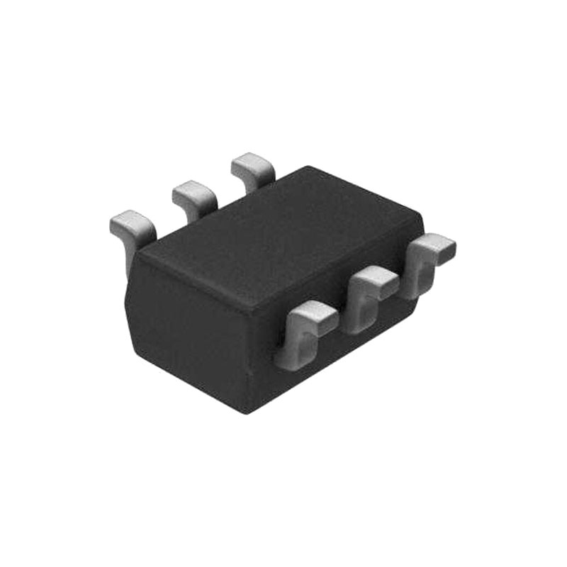
The LT1933 is a current mode PWM step-down DC/DC converter with an internal 0.75A power switch, packaged in a tiny 6-lead SOT-23. The wide input range of 3.6V to 36V makes the LT1933 suitable for regulating power from a wide variety of sources, including unregulated wall transformers, 24V industrial supplies and automotive batteries. Its high operating frequency allows the use of tiny, low cost inductors and ceramic capacitors, resulting in low, predictable output ripple.
Cycle-by-cycle current limit provides protection against shorted outputs, and soft-start eliminates input current surge during start up. The low current (<2μA) shutdown provides output disconnect, enabling easy power management in battery-powered systems.
ОСОБЕННОСТИ
Широкий диапазон входных сигналов: 3,6 - 36 В
5V at 600mA from 16V to 36V Input
3.3V at 600mA from 12V to 36V Input
5V at 500mA from 6.3V to 36V Input
3.3V at 500mA from 4.5V to 36V Input
Fixed Frequency 500kHz Operation
Uses Tiny Capacitors and Inductors
Мягкий старт
Internally Compensated
Low Shutdown Current: <2μA
Output Adjustable Down to 1.25V
Low Profi le (1mm) SOT-23 (ThinSOT™) and (2mm × 3mm × 0.75mm) 6-Pin DFN Packages
ПРИЛОЖЕНИЯ
Регулирование автомобильных аккумуляторов
Промышленные принадлежности для управления
Регулировка настенного трансформатора
Регулирование распределенного снабжения
Battery-Powered Equipment
ОПЕРАЦИЯ
The LT1933 is a constant frequency, current mode step down regulator. A 500kHz oscillator enables an RS fl ipfl op, turning on the internal 750mA power switch Q1. An amplifi er and comparator monitor the current fl owing between the VIN and SW pins, turning the switch off when this current reaches a level determined by the voltage at VC. An error amplifi er measures the output voltage through an external resistor divider tied to the FB pin and servos the VC node. If the error amplifi er’s output increases, more current is delivered to the output; if it decreases, less current is delivered. An active clamp (not shown) on the VC node provides current limit. The VC node is also clamped to the voltage on the SHDN pin; soft-start is implemented by generating a voltage ramp at the SHDN pin using an external resistor and capacitor.
An internal regulator provides power to the control circuitry. This regulator includes an undervoltage lockout to prevent switching when VIN is less than ~3.35V. The SHDN pin is used to place the LT1933 in shutdown, disconnecting the output and reducing the input current to less than 2μA.
The switch driver operates from either the input or from the BOOST pin. An external capacitor and diode are used to generate a voltage at the BOOST pin that is higher than the input supply. This allows the driver to fully saturate the internal bipolar NPN power switch for effi cient operation.
The oscillator reduces the LT1933’s operating frequency when the voltage at the FB pin is low. This frequency foldback helps to control the output current during startup and overload.
ИНФОРМАЦИЯ О ПРИЛОЖЕНИЯХ
FB Resistor Network
The output voltage is programmed with a resistor divider between the output and the FB pin. Choose the 1% resistors according to:
R1 = R2(VOUT/1.245 – 1)
R2 should be 20k or less to avoid bias current errors.
Input Voltage Range
The input voltage range for LT1933 applications depends on the output voltage and on the absolute maximum ratings of the VIN and BOOST pins.
The minimum input voltage is determined by either the LT1933’s minimum operating voltage of ~3.35V, or by its maximum duty cycle. The duty cycle is the fraction of time that the internal switch is on and is determined by the input and output voltages:
DC = (VOUT + VD)/(VIN – VSW + VD)
where VD is the forward voltage drop of the catch diode (~0.4V) and VSW is the voltage drop of the internal switch (~0.4V at maximum load). This leads to a minimum input voltage of:
VIN(MIN) = (VOUT + VD)/DCMAX – VD + VSW
with DCMAX = 0.88
The maximum input voltage is determined by the absolute maximum ratings of the VIN and BOOST pins and by the minimum duty cycle DCMIN = 0.08 (corresponding to a minimum on time of 130ns):
VIN(MAX) = (VOUT + VD)/DCMIN – VD + VSW
Note that this is a restriction on the operating input voltage; the circuit will tolerate transient inputs up to the absolute maximum ratings of the VIN and BOOST pins.

