ОПИСАНИЕ
The LT1997-3 combines a precision operational amplifier with highly-matched resistors to form a one-chip solution for accurately amplifying voltages. Gains from –13 to +14 with accuracy of 0.006% (60ppm) can be achieved using no external components. The LT1997-3 is particularly well suited for use as a difference amplifier, where the excellent resistor matching results in a common mode rejection ratio of greater than 91dB.
The amplifier features a 60μV maximum input offset voltage and a –3dB bandwidth of 1.1MHz (Gain = 1). The LT1997-3 operates from any supply voltage from 3.3V to 50V and draws only 350μA supply current. The output typically swings to within 100mV of either supply rail.
The resistors maintain their excellent matching over temperature; the matching temperature coefficient is guaranteed less than 1ppm/°C. The resistors are extremely linear with voltage, resulting in a gain nonlinearity of less than 2ppm.
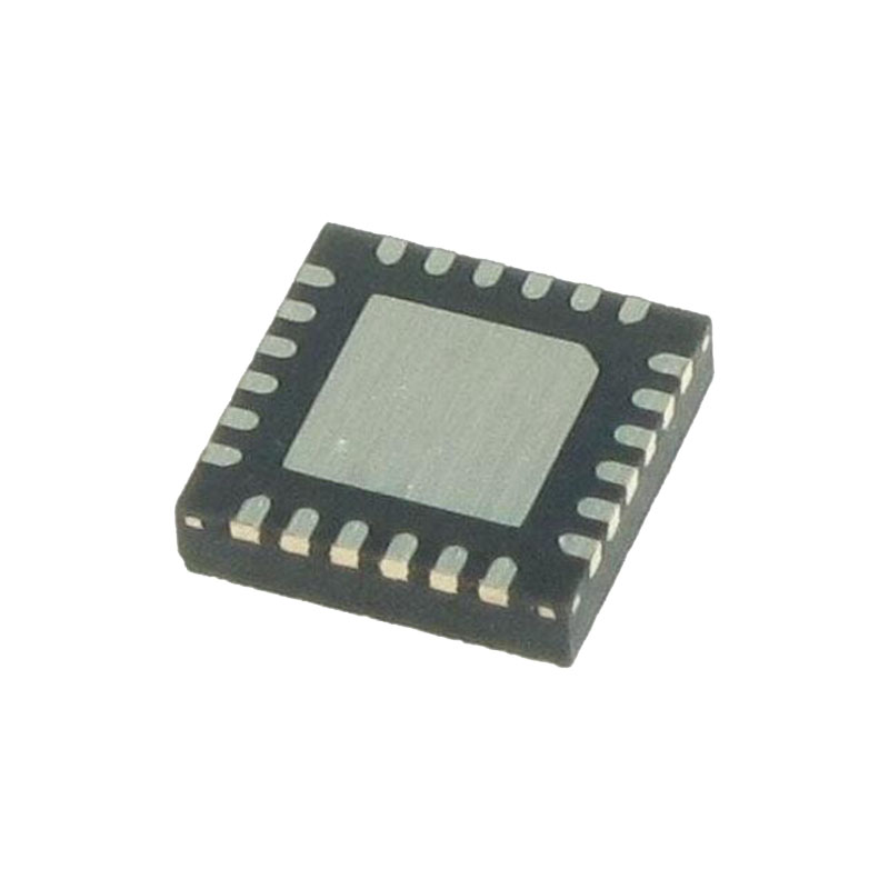
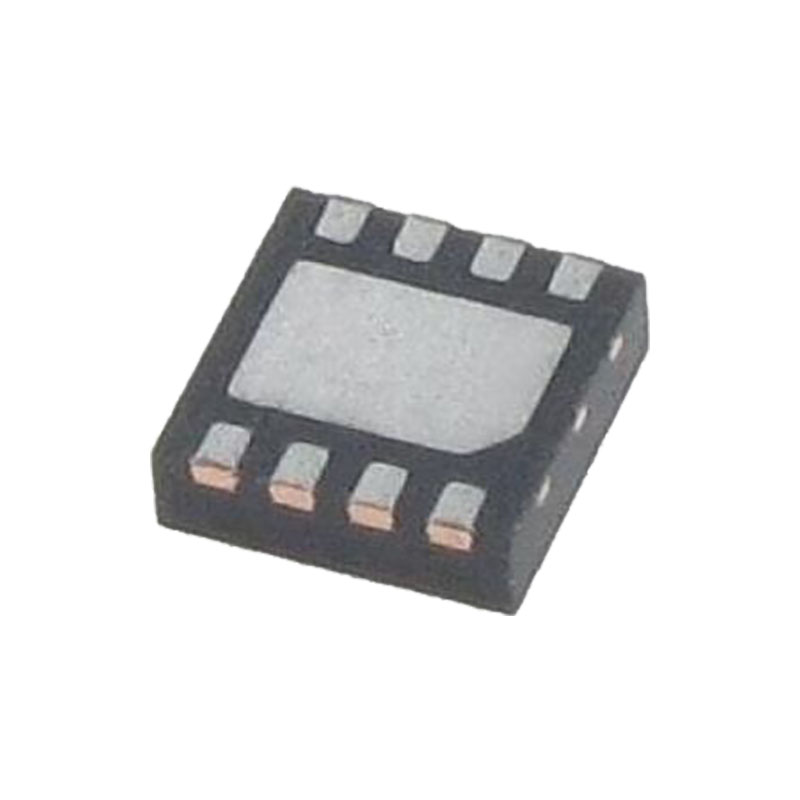
The LT1997-3 is fully specified at 5V and ±15V supplies and from –40°C to 125°C. The device is available in space saving 16-lead MSOP and 4mm × 4mm DFN14 packages.
ОСОБЕННОСТИ
Pin Configurable as a Difference Amplifier, Inverting Amplifier or Noninverting Amplifier
91dB Minimum DC CMRR (Gain = 1)
65dB AC CMRR (at 100kHz, Gain = 1)
0.006% (60ppm) Maximum Gain Error (Gain = 1)
1ppm/°C Maximum Gain Error Drift
2ppm Maximum Gain Nonlinearity
±160V Common Mode Voltage Range
Wide Supply Voltage Range: 3.3V to 50V
Выход "рельс в рельс
350μA Supply Current
60μV Maximum Op Amp Offset Voltage
1.1MHz –3dB Bandwidth (Gain = 1)
Low-Power Shutdown: 20μA
Space-Saving MSOP and DFN Packages
ПРИЛОЖЕНИЯ
High Side or Low Side Current Sensing
Bidirectional Wide Common Mode Range Current Sensing
High Voltage to Low Voltage Level Translation
Industrial Data-Acquisition Front-Ends
Replacement for Isolation Circuits
Differential to Single-Ended Conversion
ИНФОРМАЦИЯ О ПРИЛОЖЕНИЯХ
Introduction The LT1997-3 is a precision, high voltage general purpose op amp combined with a highly-matched resistor network. It can easily be configured into many different classical gain circuits without adding external components. The several pages of simple circuits in this data sheet demonstrate how easy the LT1997-3 is to use. It can be configured into a difference amplifier (Figure 1), as well as into inverting (Figure 7) and noninverting (Figure 3) single ended amplifiers. The LT1997-3 provides the resistors and op amp together in a small package in order to save board space and reduce complexity. Highly accurate measurement circuits can be easily constructed with the LT1997-3. The circuits can be tailored to specific measurement applications.
Common Mode Voltage Range The common mode voltage range of the LT1997-3 is set by the voltage range allowed on the LT1997-3’s input pins and by the input voltage range of the internal op amp. The internal op amp of LT1997-3 has 2 operating regions: a) if the common-mode voltage at the inputs of the internal op amp (VCMOP) is between V– and V+ – 1.75V, the op amp operates in its normal region; b) If VCMOP is between V+ – 1.75V and V– + 76V, the op amp continues to operate, but in its Over-The-Top (OTT) region with degraded performance.
The LT1997-3 will not operate correctly if the commonmode voltage at the inputs of the internal op amp (VCMOP) is below V–, but the part will not be damaged as long as VCMOP is greater than V– – 25V and the junction temperature of the LT1997-3 does not exceed 150ºC.
The allowed voltage range on LT1997-3’s input pins are as follows: The voltages at +INA and –INA input pins should never be higher than V– + 160V or lower than V– – 160V under any circumstances; The voltages at +INB, –INB, +INC and –INC input pins should not go below V– – 0.3V or above V– + 80V.
The common-mode voltage at the inputs of the internal op amp (VCMOP) is determined by the voltages on pins +INA, +INB, +INC and REF (see the “Calculating Input Voltage Range” section). This condition is true provided that the internal op amp’s output is not clipped and feedback maintains the internal op amp’s inputs at the same voltage.
In addition to the limits mentioned above, the common mode input voltage of the amplifier should be chosen so that the input resistors do not dissipate too much power. The power dissipated in a 22.5k resistor must be less than 1.5W. It must be less than 0.5W for the 7.5k resistor and less than 0.165W for the 2.5k resistor. For most applications, the pin voltage limitations will be reached before the resistor power limitation is reached.