ОПИСАНИЕ
The LT8610A/LT8610AB series are compact, high efficiency, high speed synchronous monolithic step-down switching regulators that consume only 2.5µA of quiescent current. Compared to the LT8610, they have higher maximum output currents of 3.5A and a faster minimum switch-on time of 30ns. The LT8610A has the same low ripple burst mode performance of the LT8610, while the LT8610AB has even higher light load efficiency.
The other features of the LT8610 remain unchanged in the LT8610A/LT8610AB series. A SYNC pin allows synchronization to an external clock. The EN/UV pin has an accurate 1V threshold for VIN undervoltage lockout or shut down. A capacitor on the TR/SS pin programs the output voltage ramp rate during startup. The PG flag signals when VOUT is within ±9% of the programmed output voltage as well as fault conditions.
ОСОБЕННОСТИ
LT8610 Feature Set, Plus:
3.5A Maximum Output Current
Fast 30ns Minimum Switch-On Time
Improved Burst Mode Efficiency (LT8610AB Only) Improved EMI
Wide Input Voltage Range: 3.4V to 42V
Ultralow Quiescent Current Burst Mode® Operation: 2.5μA IQ Regulating 12VIN to 3.3VOUT
Fixed Output Voltages: 3.3V, 5V
Output Ripple < 10mVP-P (LT8610A Only)
High Efficiency Synchronous Operation:
95% Efficiency at 1A, 5VOUT from 12VIN
93% Efficiency at 1A, 3.3VOUT from 12VIN
Low Dropout Under All Conditions: 200mV at 1A
Safely Tolerates Inductor Saturation in Overload
Adjustable and Synchronizable Frequency: 200kHz to 2.2MHz
Accurate 1V Enable Pin Threshold
Output Soft-Start and Tracking
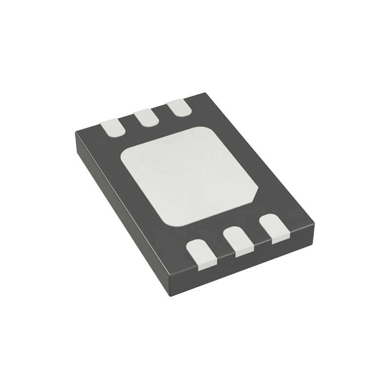
Small Thermally Enhanced 16-Lead MSOP Package
Квалификация AEC-Q100 для применения в автомобильной промышленности
ПРИЛОЖЕНИЯ
Automotive and Industrial Supplies
GSM Power Supplies
ОПЕРАЦИЯ
The LT8610A/LT8610AB is a monolithic, constant frequency, current mode step-down DC/DC converter. An oscillator, with frequency set using a resistor on the RT pin, turns on the internal top power switch at the beginning of each clock cycle. Current in the inductor then increases until the top switch current comparator trips and turns off the top power switch. The peak inductor current at which the top switch turns off is controlled by the voltage on the internal VC node. The error amplifier servos the VC node by comparing the voltage on the VFB pin with an internal 0.97V reference. When the load current increases it causes a reduction in the feedback voltage relative to the reference leading the error amplifier to raise the VC voltage until the average inductor current matches the new load current. When the top power switch turns off, the synchronous power switch turns on until the next clock cycle begins or inductor current falls to zero. If overload conditions result in more than 3.3A flowing through the bottom switch, the next clock cycle will be delayed until switch current returns to a safe level.
ИНФОРМАЦИЯ О ПРИЛОЖЕНИЯХ
Achieving Ultralow Quiescent Current
To enhance efficiency at light loads, the LT8610A/LT8610AB operates in low ripple Burst Mode operation, which keeps the output capacitor charged to the desired output voltage while minimizing the input quiescent current and minimizing output voltage ripple. In Burst Mode operation the LT8610A/LT8610AB delivers single pulses of current to the output capacitor followed by sleep periods where the output power is supplied by the output capacitor. While in sleep mode the LT8610A/LT8610AB consumes 1.7μA.
Shorted and Reversed Input Protection
The LT8610A/LT8610AB will tolerate a shorted output. Several features are used for protection during output short-circuit and brownout conditions. The first is the switching frequency will be folded back while the output is lower than the set point to maintain inductor current control. Second, the bottom switch current is monitored such that if inductor current is beyond safe levels switching of the top switch will be delayed until such time as the inductor current falls to safe levels.