ОПИСАНИЕ
The LTC3569 contains three monolithic, synchronous step-down DC/DC converters. Intended for medium power applications, it operates over a 2.5V to 5.5V input voltage range. The operating frequency is adjustable from 1MHz to 3MHz, allowing the use of tiny, low cost capacitors and inductors. The three output voltages are independently programmable by toggling the EN pins up to 15 times, lowering the 800mV FB references by 25mV per cycle. The first buck regulator sources load currents up to 1200mA. The other two buck regulators each provide 600mA.
The two 600mA buck regulators can also be configured to operate as slave power stages, running in parallel with another internal buck regulator to supply higher load currents. When operating as parallel, slave output stages, discrete external components are shared and available output currents sum together.
ОСОБЕННОСТИ
Three Independent Current Mode Buck DC/DC Regulators (1.2A and 2 × 600mA)
Single Pin Programmable VFB Servo Voltages from 800mV Down to 425mV (in 25mV Steps)
Pull VFB High to Make Each 600mA Buck a Slave for Higher Current Operation
Pulse-Skipping or Burst Mode® Operation
Programmable Switching Frequency (1MHz to 3MHz) or Fixed 2.25MHz
Synchronizable (1.2MHz to 3MHz)
VIN Range 2.5V to 5.5V
All Regulators Internally Compensated
PGOOD Output Flag
Quiescent Current <100µA (All Regulators in Burst Mode Operation)
Zero Shutdown Current
Overtemperature and Short-Circuit Protection
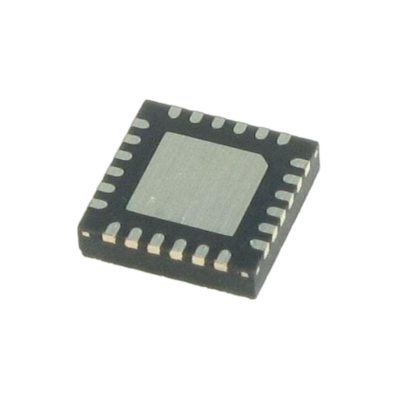
Tiny 3mm × 3mm, 3mm × 4mm 20-Lead QFN and Thermally Enhanced TSSOP FE-16 Packages
ПРИЛОЖЕНИЯ
Portable Applications with Multiple Supply Rails
General Purpose Step-Down DC/DC
Dynamic Voltage Scaling Applications
ОПЕРАЦИЯ
Introduction
The LTC3569 contains three constant-frequency, current mode buck DC/DC regulators. Both the P-channel and synchronous rectifier (N-channel) switches are internal to each buck. The operating frequency is determined by the value of the RT resistor, or is fixed to 2.25MHz by pulling the RT pin to SVIN, or is synchronized to an external oscillator tied to the MODE pin. Users may select pulseskipping or Burst Mode operation to trade off output ripple for efficiency. Independent programmable reference levels allow the LTC3569 to suit a variety of applications.
The LTC3569 offers different power levels, a single 1.2A buck as well as two 600mA bucks. These three bucks may be configured in different parallel configurations, for versatile high current operation. The power stage of buck 2 can be configured as a slave to buck 1, by pulling FB2 to SVIN. The power stage of buck 3, can be configured to be a slave to buck 2, by pulling the FB3 pin to SVIN. To enable the slave power stage, pull the respective EN pin high. However if the master is disabled, the slave power stage is Hi-Z.
Low Current Operation
At light loads, the FB voltage may rise above the reference voltage. If this occurs the error amplifier signals the control loop to go to sleep, and the P-channel turns off immediately. The inductor current then discharges through the N-channel switch until the inductor current approaches zero; whereupon the SW goes Hi-Z, and the output capacitor supplies power to the load. When the load discharges the output capacitor the feedback voltage falls and the error amp wakes up the buck, restarting the main control loop as if a clock cycle has just begun. This sleep cycle helps minimize the switching losses which are dominated by the gate charge losses of the power devices. Two operating modes are available to control the operation of the LTC3569 at low currents, Burst Mode operation and pulse-skipping mode.
Select Burst Mode operation to optimize efficiency at low output currents. In Burst Mode operation the inductor current reaches a fixed current before the P-channel switch compares inductor current against the value determined by ITH. This burst clamp causes the output voltage to rise above the regulation voltage and forces a longer sleep cycle. This greatly reduces switching losses and average quiescent current at light loads, at the cost of higher ripple voltage.