Описание
The Microchip Technology Inc. MCP6001/2/4 family of operational amplifiers (op amps) is specifically designed for general purpose applications. This family has a 1 MHz Gain Bandwidth Product (GBWP) and 90° phase margin (typical). It also maintains a 45° phase margin (typical) with a 500 pF capacitive load. This family operates from a single-supply voltage as low as 1.8V, while drawing 100 µA (typical) quiescent current.Additionally, the MCP6001/2/4 supports rail-to-rail input and output swing, with a Common-mode input voltage range of VDD + 300 mV to VSS – 300 mV. This family of op amps is designed with Microchip’s advanced CMOS process.
The MCP6001/2/4 family is available in the industrial and extended temperature ranges, with a power supply range of 1.8V to 6.0V.
Характеристики
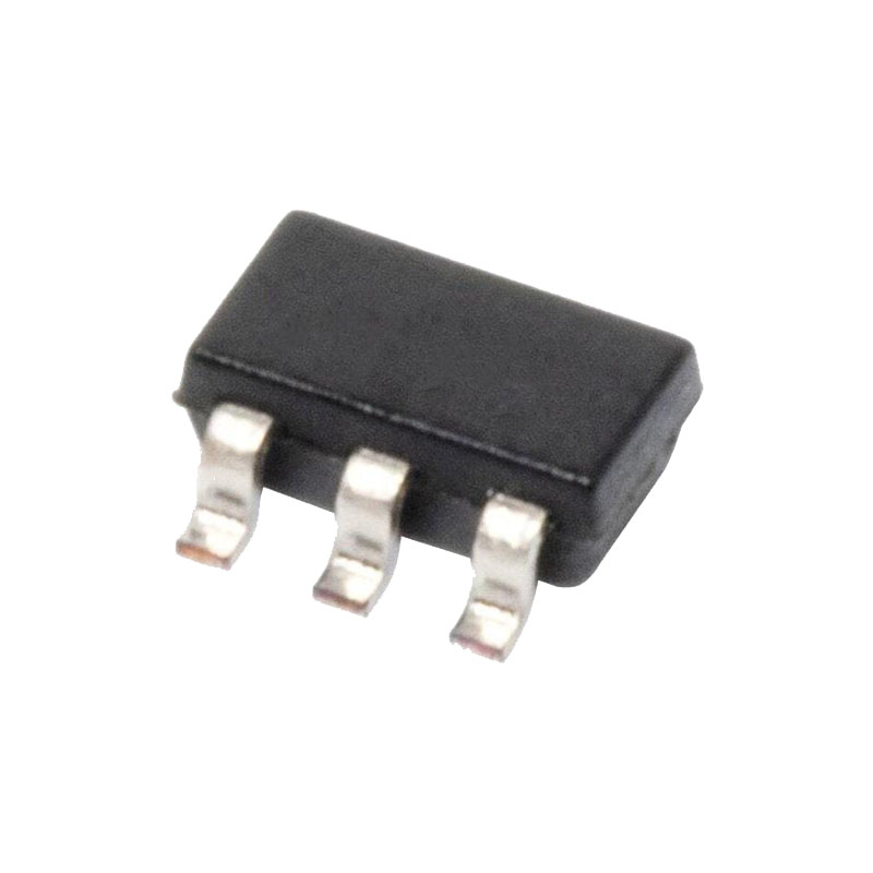
• Available in 5-Lead SC-70 and 5-Lead SOT-23 Packages
• Gain Bandwidth Product: 1MHz (typical)
• Rail-to-Rail Input/Output
• Supply Voltage: 1.8V to 6.0V
• Supply Current: IQ = 100µA (typical)
• Phase Margin: 90° (typical)
• Temperature Range:
– Industrial: -40°C to +85°C
– Extended: -40°C to +125°C
• Available in Single, Dual and Quad Packages
Приложения
• Automotive
• Portable Equipment
• Photodiode Amplifier
• Analog Filters
• Notebooks and PDAs
• Battery-Powered Systems
Design Aids
• SPICE Macro Models
• FilterLab Software
• Mindi™ Circuit Designer and Analog Simulator
• Microchip Advanced Part Selector (MAPS)
• Analog Demonstration and Evaluation Boards
• Application Notes
Power Supply Pins
The positive power supply (VDD) is 1.8V to 6.0V higher than the negative power supply (VSS). For normal operation, the other pins are at voltages between VSS and VDD.
Typically, these parts are used in a single (positive) supply configuration. In this case, VSS is connected to ground and VDD is connected to the supply. VDD will need bypass capacitors.
APPLICATION INFORMATION
The MCP6001/2/4 family of op amps is manufactured using Microchip’s state-of-the-art CMOS process and is specifically designed for low-cost, low-power and general purpose applications. The low supply voltage, low quiescent current and wide bandwidth makes the MCP6001/2/4 ideal for battery-powered applications. These devices have high phase margin, which makes them stable for larger capacitive load applications.
Capacitive Loads
Driving large capacitive loads can cause stability problems for voltage feedback op amps. As the load capacitance increases, the feedback loop’s phase margin decreases and the closed-loop bandwidth is reduced. This produces gain peaking in the frequency response, with overshoot and ringing in the step response. While a unity gain buffer (G = +1) is the most sensitive to capacitive loads, all gains show the same general behavior.
Unused Op Amps
An unused op amp in a quad package (MCP6004) should be configured. These circuits prevent the output from toggling and causing crosstalk. Circuit A sets the op amp at its minimum noise gain. The resistor divider produces any desired reference voltage within the output voltage range of the op amp; the op amp buffers that reference voltage. Circuit B uses the minimum number of components and operates as a comparator, but it may draw more current.
ACTIVE LOW-PASS FILTER
The MCP6001/2/4 op amp’s low input bias current makes it possible for the designer to use larger resistors and smaller capacitors for active low-pass filter applications. However, as the resistance increases, the noise generated also increases. Parasitic capacitances and the large value resistors could also modify the frequency response. These trade-offs need to be considered when selecting circuit elements.
Usually, the op amp bandwidth is 100x the filter cutoff frequency (or higher) for good performance. It is possible to have the op amp bandwidth 10x higher than the cutoff frequency, thus having a design that is more sensitive to component tolerances.
SPICE Macro Model
The model covers a wide aspect of the op amp’s electrical specifications. Not only does the model cover voltage, current and resistance of the op amp, but it also covers the temperature and noise effects on the behavior of the op amp. The model has not been verified outside of the specification range listed in the op amp data sheet. The model behaviors under these conditions can not be ensured that it will match the actual op amp performance.

